AFM has been used for decades to not only image a material, but to also measure their nanoelectrical properties. AFM instruments can be used on a wide range of materials, but recent advancements in AFM technologies has allowed for more information to be obtained, and “softer” materials to be analyzed.
Seminar overview
The webinar will look at how AFM-based nanoelectrical measurement capability has advanced, how it is now more accessible to a wider range of materials and how the user can obtain a greater amount of information about their sample than has previously been possible. The properties which can be measured by current AFM instruments will be compared to Bruker’s new state-of-the-art solution.
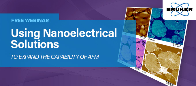
The webinar will showcase how correlating nanomechanical and nanoelectrical measurements can lead to a greater determination of properties. It aims to show how Bruker’s new solution, the NanoElectrical Lab, can correlate both the mechanical and electrical data at each single pixel for an increased understanding of sample properties and an increase in the longevity of AFM tips.
What to expect
The webinar will look at the recent advancements made by Bruker to correlate electrical and mechanical measurements at every pixel with the new DataCube modes, offering comprehensive and reliable analysis. It will also look at how Bruker’s new solution reduces sample and tip damage and will showcase new applications revealed with these modes.
Key topics
The NanoElectrical Lab:
- Introduction to NEW DataCube modes
- Correlation of nanomechanical and nanoelectrical data
- Possibilities for tailored nanoelectrical measurements
Applications:
- Graphene and other 2D materials
- Semiconductors
- Nanowires
- Electrics
- Smart materials
- Conductive polymers
- Batteries
- Fuel Cells
Who should attend?
Overall, this webinar is tailored to those who already undertake electrical measurements, or are interested in it, as well as people who are already using existing techniques but require a higher resolution. In addition, it will be of interest to people who already use AFM but not necessarily for nanoelectrical measurements. General microscopists who are interested in measuring properties at the nanometer scale will also be interested in this webinar.
Presenter Biographical
Dr Peter DeWolf graduated from The University of Ghent with a degree in Electrical Engineering and followed this with a PhD from KU Leuven University. Since then, Peter has been authored on 47 academic publications focused around microscopy techniques. He is now the Application Director for Nano Surfaces Business at Bruker.